|
 Home > Company Profile > Business Areas > Plant >
Processed goods
Home > Company Profile > Business Areas > Plant >
Processed goods |
 |
| |
 |
| |
|
|
| |
|
| Model |
Image |
Description |
| BGA |
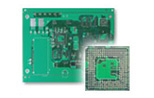 |
One of large scale integrated circuit. Put LSI bare chip On the Square PCB and array domed terminal with the shape of two-dimensional array on the back. Terminal treats with solder. Package of 225~460 pin has been put to practical use. Recently, it is watched because LSI package taking a lot of terminals can be miniaturized. The fact that ˇ®MotorolaˇŻ used it to beeper by developing made it spread. Today, it is used to semiconductor on demand (ASIC) high-speed passive Ram (SRAM) as a package. Recently, the shape has been diversified and kinds based on ceramic and plastic tape (TAB tape) were developed. Kinds using 4~6 multilayers have been developed except both-sided board.
|
| MLB |
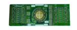 |
-As a stereoscopic PCB having inside and outside circuits, this is a product that able to decrease high density part insertion and wiring distance by stereoscopic wiring.
- Application : Used to mainly large computer, PC, communication
equipment , small appliances |
| HDI |
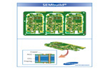 |
High Density Interconnect
˘ˇAs a process confronting with high density & multilayer with fast-growing telecommunication industry, this is a multilayer product of new manufacturing process making layers by stages, Micro Via and Fine Pattern out of multilayer by the existing laminated method.
|
| FCBGA |
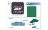 |
Filp Chip Ball Grid Arrays
˘ˇ Packaging technology using Ball instead of Pin(PGA) or Lead(QFP) when attaching Packaging. Strong to noise because area of part exterior terminal does not protrude. Also, size of approximately 50% became smaller because pin does not protrude. |
|
| |
| |
|
| |
| |
|